
Over the summer of 2026, the pro² network+ organised a call seeking projects that enabled more environmentally sustainable production of digital devices. Included within the scope of the call were ways of reducing environmental impact through sustainable design and production processes, responsible sourcing of components, and minimising impact during device operation and at end-of-life.
Ultimately two projects were successful in responding to the call. Launching in the autumn of 2026, these projects will offer new solutions to empower the sustainable low-volume production of digital devices.
REINCARNATE: Evidence-Led Recovery and Reuse of Retired Electronic Components
Electronic waste, or e-waste, is one of the fastest growing waste streams, having produced a record 62 million tonnes globally in 2022. Of that amount, only about 22% was known to be collected and recycled, despite the materials embedded in that year’s waste valuing in at around $91 billion US dollars. In many cases devices are discarded due to a deployment ending or specification change rather than failure, resulting in the disposal of working components.
This project will build and demonstrate a complete route from a retired device to a newly built one, in which a sequence of AI models and a controlled bench study work together to decide what is worth recovering and what can be made from it. Vision models will screen each board for damage and identify its components; existing compliance and market databases will attach each part’s regulatory status and value; and a controlled desolder-and-test study will measure on a real deployed device how long each component takes to remove, how often it survives removal, and whether it still works afterwards. That measured evidence is the data the field has lacked: it replaces the assumed recovery figures in techno-economic models with measured ones. A decision step then fuses removal cost, survival, hazard, and value into a board-level recovery strategy, and a constraint-based recipe step takes the confirmed inventory of recovered, tested parts and returns a buildable low-power device, with a schematic, a bill of materials, and the few new parts needed to complete it.
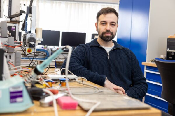
The project is led by Dr Oktay Cetinkaya, a Lecturer in Electronic Systems at the University of Manchester. It is further supported by industry partner Connexin Limited, a smart-technology and digital-infrastructure provider that runs one of the UK’s largest LoRaWAN networks.
Reconfigurable and Repairable Electronics for Circular Device Prototyping
Traditional iterative prototyping processes used to develop digital devices often contribute to the growing international problem of e-waste. Printed circuit board (PCB) fabrication, for example, requires energy-intensive manufacturing processes, chemically processed materials, and often overseas manufacture, and typically result in single-use prototypes that are discarded after each iteration. Options like breadboards and perfboards may limit innovation due to their rigid grid configuration, and in the case of the latter, the wiring connections generate additional e-waste. Even after the development phase, devices are often discarded due to issues like a lack of repairability, thus shortening a device’s lifespan and leading to greater waste.
This project will develop a solution by creating a circular prototyping platform for digital device development based on reusable, low-melting-point conductive metals such as Field’s metal. The platform enables rapid fabrication, reconfiguration, and repair of electronic systems through fully recoverable conductive architectures and a direct-write deposition approach, allowing circuits to be created, modified, and restored without generating material waste. A circuit can be drawn onto a substrate by melting and solidifying Field’s metal (melting point 62°C). Electronic components can be placed into position and the connection to the circuit achieved by melting then solidifying Field’s metal (no solder required). The circuit can be modified by selectively melting Field’s metal, then adding or removing components or conductive traces. At the end of the lifetime, the Field’s metal circuit can be melted and recovered and all electronic components reused.
-
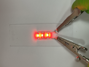
- A functioning circuit formed by solidified Field’s metal conductors.
-
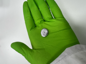
- A solidified Field’s metal droplet.
The project is led by Professor Yi Wang of the Emerging Device Technology research lab at the University of Birmingham. The team also includes Dr Tim Cole (U. of Birmingham) and Associate Professor Shiyang Tang of the University of Southampton.
What’s next?
If you’re curious to know more about these projects, follow us on LinkedIn, Bluesky, and Instagram for updates. You can also register for free to be a pro² network+ member, giving you access to the member’s section of our website for networking and collaboration. Members also receive the pro² newsletter with information about our events, future funding calls, and everything we’re doing to democratise the production of digital devices.